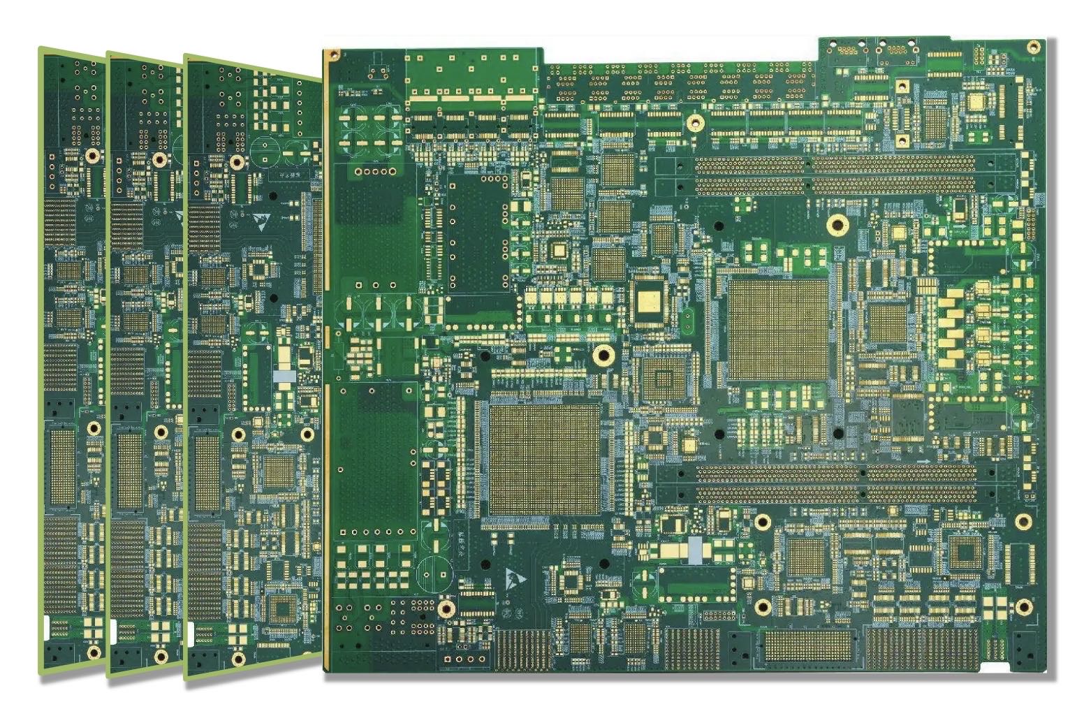
In the competitive electronics market of 2026, every cent counts. Whether you are a startup launching a Kickstarter campaign or an established enterprise managing a supply chain, optimizing your Bill of Materials (BOM) is critical.
However, cutting costs in PCB manufacturing doesn’t mean switching to the cheapest vendor who might use inferior materials. It is about Design for Manufacturing (DFM). By optimizing your design to align with standard manufacturing capabilities, you can significantly lower your unit price without risking reliability.
Here is how you can optimize your design for cost-efficiency.
📐 Optimize Panel Size and Utilization
The most fundamental way to reduce cost is to maximize the usage of the raw material. PCB manufacturers typically work with standard production panels (e.g., 18″ x 24″ or 21″ x 24″).
- Minimize Board Dimensions: Every square millimeter counts. In the design phase, review your board outline. Can the PCB be made slightly smaller to fit more units into a standard panel? Reducing the board size by even a few millimeters can allow for an extra column of boards per panel, drastically dropping the cost per unit in mass production.
- Design for Panelization: If your board is small, design it with panelization in mind. Avoid complex, irregular shapes (circles or odd angles) that leave large gaps of wasted material between boards. Rectangular or square boards pack together most efficiently.
- Avoid Complex Cutouts: Internal cutouts and slots require routing or laser cutting, which takes more machine time than standard V-scoring or tab-routing. Unless necessary for the enclosure, stick to a simple outer profile.
📉 Reduce Layer Count and Complexity
Layer count is one of the biggest drivers of PCB cost. Moving from a 4-layer board to a 6-layer board doesn’t just add two layers of material; it increases the complexity of lamination, drilling, and alignment.
- Challenge Your Layer Count: Do you really need 8 layers? Often, a layout engineer can route a design on 6 layers with tighter trace rules. While this requires more design effort, the manufacturing savings are substantial.
- Simplify Routing: By using slightly thinner traces (within the manufacturer’s capability) and optimizing component placement, you can often reduce the required layer count.
- Minimize Blind/Buried Vias: Standard through-hole vias are cheap. Blind and buried vias require complex sequential lamination processes. Unless you are designing for a high-density smartphone or FPGA, stick to through-hole vias to keep processing costs low.
🧪 Select Standard Materials and Finishes
Not all PCB materials are created equal, and neither are their price tags. Choosing “good enough” materials for your specific application is key.
- Stick to Standard FR-4: Unless your product operates in extreme temperatures or high-frequency environments (like 5G or RF applications), standard FR-4 (TG130-TG150) is the most cost-effective choice. Avoid high-TG or halogen-free materials unless explicitly required by your client or regulations.
- Choose the Right Surface Finish:
- HASL (Lead-Free): This is generally the cheapest option. It is durable and easy to solder, making it perfect for consumer electronics where fine-pitch components are not used.
- ENIG (Gold): While ENIG offers a flat surface ideal for fine-pitch chips and wire bonding, it is significantly more expensive. Only use ENIG if your components specifically require the flatness or if you need the corrosion resistance for harsh environments.
- Standard Copper Weight: Stick to 1oz (35µm) copper for signal layers. Using 2oz or heavier copper increases etching time and cost. Only use heavy copper on power planes where high current is actually present.
🛠️ Follow Standard Design Rules (DFM)
Manufacturing costs spike when a board requires “special handling.” By adhering to standard capabilities, you ensure your board flows through the factory quickly and efficiently.
- Avoid “Via-in-Pad”: Placing a via directly on a component pad (Via-in-Pad) saves space but requires the via to be filled and plated over. This adds multiple processing steps. If space permits, use standard “dog-bone” fan-outs instead.
- Relax Tolerances: Do not specify tight tolerances (e.g., ±0.05mm) unless absolutely necessary for impedance control or connector fit. Standard tolerances (±0.1mm) are easier and cheaper to manufacture.
- Standardize Hole Sizes: Reduce the number of different drill sizes in your design. Every unique drill size requires a tool change on the drilling machine. Using a standard set of hole sizes (e.g., 0.3mm, 0.8mm) speeds up production.
⚖️ Cost Optimization Comparison
To visualize the impact of these decisions, refer to the table below:
表格
| Feature | High Cost Choice | Cost-Effective Choice |
|---|---|---|
| Board Shape | Circular / Complex Cutouts | Rectangular / Simple Outline |
| Via Type | Blind / Buried / Via-in-Pad | Through-Hole Vias |
| Surface Finish | ENIG (Gold) / Immersion Silver | HASL (Lead-Free) |
| Material | Rogers / High-TG FR-4 | Standard FR-4 (TG130) |
| Tolerance | Class 3 (Aerospace/Medical) | Class 2 (Consumer/Industrial) |
Pro Tip: Always consult with your PCB manufacturer’s engineering team before finalizing your design. A quick DFM review can identify cost-saving opportunities that software might miss.
By implementing these strategies, you aren’t just “cutting costs”—you are designing a smarter, more manufacturable product. This ensures that your electronics are not only affordable but also reliable and ready for the market.